Integrated Circuits Fabrication and their Technologies
As it was mentioned in the integrated circuits article that it is the strong body of technology and that it is better than vacuum tubes. In this article, we will show the types of integrated circuits technologies and how to manufacture them from the beginning of the sand through the silicon to the final IC.
» Integrated Circuits Technologies
The IC technology is mean that how much its size and how many transistors integrated with each other to form a single IC chip.There are many types of IC technologies as shown in the following table.
IC Technology Type | Transistors number | Application |
Small Scale Integration SSI | 1 – 100 | Logic gates, Op-Amp, Flipflops |
|
|
|
Medium Scale Integration MSI | 100 – 1000 | Counters, MUX, adders, 4bit µPs |
Large Scale Integration LSI | 1000 – 10K | 8bit µPs, ROM, RAM |
Very Large Scale Integration VLSI | 10K – 1M | 16,32bit µPs, CMOS |
Ultra Large Scale Integration ULSI | 1M – 10M | Pentium Processors |
Giant Large Scale Integration GSI | above 10M | Embedded systems, systems on chip |
» Integrated Circuits Fabrication Techniques
The fabrication of semiconductor devices is the process used to fabricate integrated circuits devices, typically metal oxide semiconductor MOS devices used in integrated circuits chips in any electrical and electronic devices. The starting material for integrated circuits fabrication is Single crystal silicon wafer. The fabrication operation is has many steps:
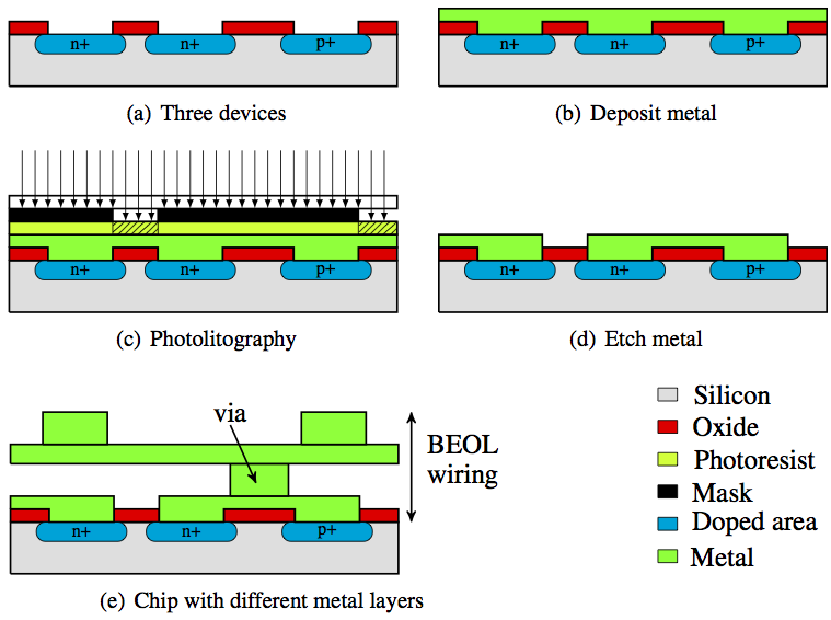
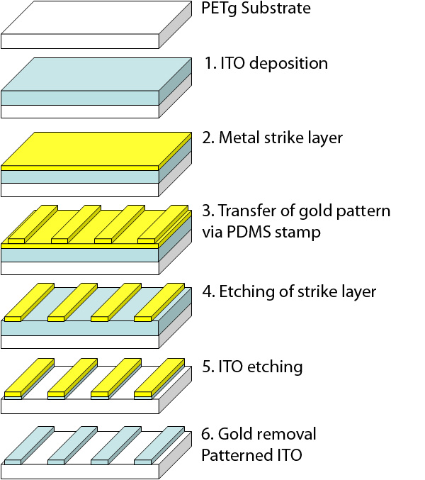
1. Layering, The layering step serves to add thin layers to the surface of the wafer. These layers may be of a different material, microstructure and composition of the same material such as polycristalline silicon and silicon oxide.
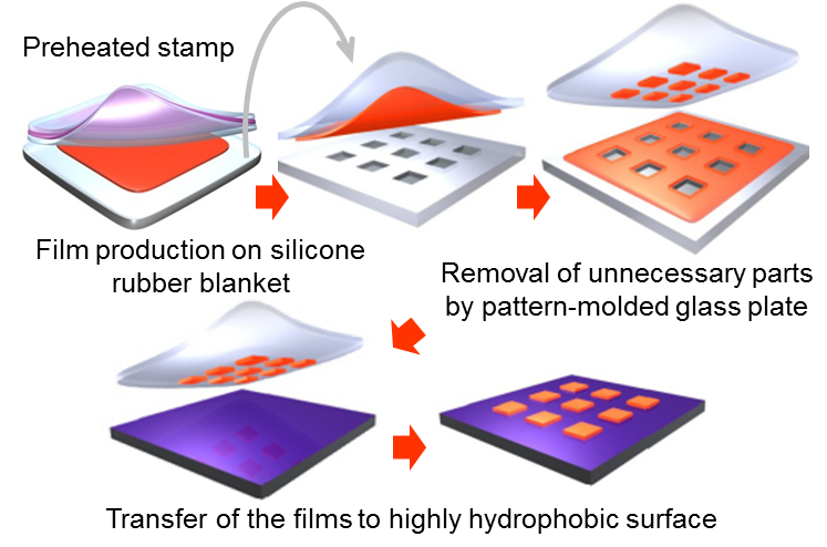
2. Patterning, the most important step in the wafer fabrication is patterning or lithography. The deposition, doping, etching and patterning refer to a series of steps to selectively mask or expose portions of the surface. It sets device’s critical dimensions on the wafers.
3. Doping, it is refers to the process of incorporating specific amounts of electrically active impurities through openings on the surface of the wafers. The doped materials are typically impurities of the type p or n and are necessary to form devices such as diodes , transistors, conductors and IC devices.
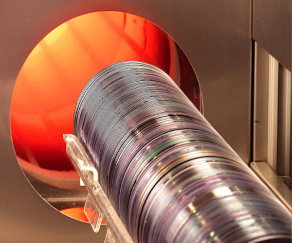
4. Heat treatment, also called Furnace annealing, it is a process used in the manufacture of semiconductor devices which consists of heating multiple wafers of semiconductors to affect their electrical properties. The heat treatments are designed for various effects. Wafers can be heated to enable dopants (doped material like phosphorus), transfer film to film or film to wafer substratum interfaces, densify deposited films, adjust grown film conditions, repair implant damage, shift dopants or drive dopants from one film to another or from a film to wafer substratum as shown in figure A.

There are many techniques of integrated circuits fabrication such as Mono-lithic, Thin Film , Thick Film and Hybrid technique. We will explain the difference between them in other article. Now, the following videos will show the journey of IC from the sand to the final IC chip.

Leave A Comment